Using Python to vectorize artwork for PCBs
The maker community has long been creating amazing art with printed circuit boards (PCB). From the incredible variety of #badgelife from folks like TwinkleTwinkie to the adorable and accessible kits from folks like Alpenglow, we've been misusing the circuit board fabrication process to great effect. I also (mis)use PCBs to create front panels for Winterbloom's modules:

Unfortunately, the process of creating these works of art with industrial processes is not easy. Getting art into a manufacturable format1 is filled with pitfalls and tedium. This has lead to some wonderful tools like svg2shenzhen, Gerbolyze, and PCBmodE- all of which are worth looking into if you want to do sort of thing.
Of course, this would be a disappointingly short and uninformative article if I just told you to go use those things. Which, by all means, if all you want to do is make art and get on with your life, then go for it! If you'd like to learn how all this works and fits together and learn how you might be able to automate parts of it, stick around!
In this article, I want to talk about just one approach for converting artwork for PCBs- Image tracing, sometimes called raster-to-vector conversion. This process takes a raster image (such a png) and converts it into a list of polygons. This article will show how I used Python to glue together a few clever libraries to build gingerbread.trace, a tool for converting images into KiCAD footprints.
The challenge
Like many EDA/CAD software packages, KiCAD works fundamentally differently from art design programs because it has a different purpose - KiCAD is for designing physical, manufacturable objects. The challenge presented here is to convert an image of some artwork into KiCAD's vector format.
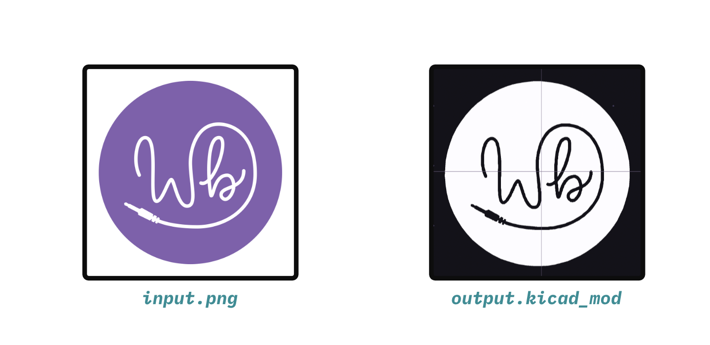
The artwork can't necessary be perfectly translated so it will have to be approximated. Luckily, KiCAD includes a GUI program called bitmap2component that can be used exactly for this purpose:
bitmap2component works but it has some drawbacks: it's a GUI program that's difficult to automate, it doesn't give you much control over the process, and it's frustrating to use with high-resolution images. Thankfully the KiCAD project is open source so it's possible learn how it works and build a similar tool that's works better for my use case.
The approach
Alright, given an image this tool needs to generate a KiCAD footprint. Looking at bitmap2component, there's a few steps it goes through to accomplish this:
- Thresholding: the image is reduced to a black & white bitmap for the following steps to work correctly.
- Tracing: An image tracing algorithm analyzes the black & white bitmap and generates a list of paths describing the filled areas in the image.
- Polygon generation: the paths are combined and transformed into polygons.
- Footprint generation: A KiCAD footprint is constructed from the polygons.
Each of these steps have some unique challenges, so I'll go through them one at a time.
Thresholding
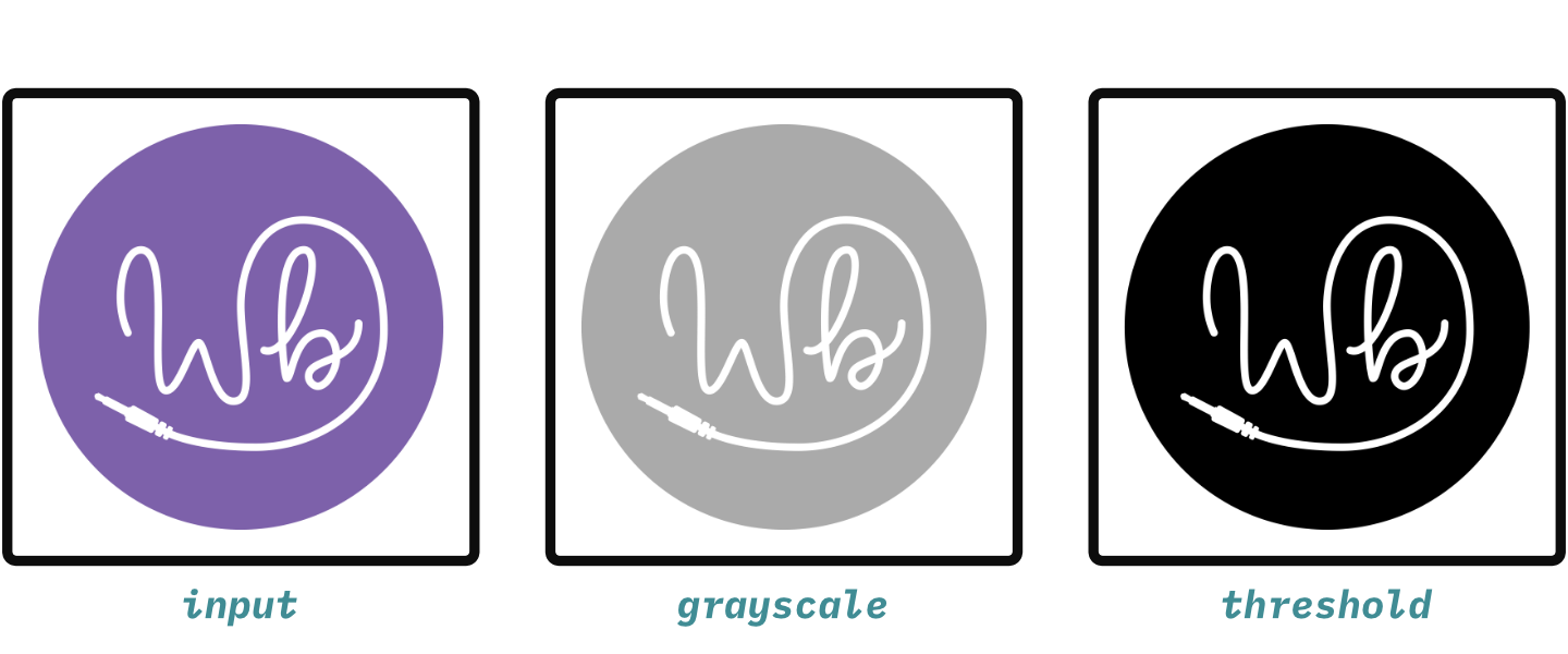
The first step is to take the image and convert it to a black & white bitmap.
While I could use the venerable Pillow to perform the image processing needed, there's an excellent, high-performance image processing library called vips that can handle large images much more efficiently. Since I want to overcome bitmap2component's frustrating experience with high-resolution images, I decided to go with vips.
The thresholding is done in a few steps. The image is first converted into 8-bit grayscale and then each pixel is compared against a threshold and set to either 255 or 0:
import pyvips

image = pyvips.Image.new_from_file("input.png")

# Remove alpha
if image.hasalpha():
    image = image.flatten(background=[255])

# Convert to black and white.
image = image.colourspace("b-w")

# Apply the threshold. Any pixels that are darker than 50% (less than 127) are
# considered filled areas, any pixels lighter than that are considered
# background. This threshold can be adjusted and inverted as needed.
image = image < 127
Here's the image at each step of the process:
Tracing
The next step is to analyze the bitmap and generate vectors. bitmap2component uses Potrace, a well established library used for image tracing.
While there are a couple of existing Python bindings to Potrace, they all fell short of exposing all the bits of Potrace I needed. I created my own bindings, potracecffi, using cffi - an excellent tool for creating bindings to C libraries.
Potrace's user interface is deceptively simple: it takes bitmap to analyze along with some optional parameters:
def trace(
    image: numpy.ndarray,
    turdsize: int = 2,
    turnpolicy: int = TURNPOLICY_MINORITY,
    alphamax: float = 1.0,
    opticurve: int = 1,
    opttolerance: float = 0.2):
This is where I ran into the first real challenge with Potrace: getting the image data into the right format. While the thresholding process converted every pixel value into a binary black or white, each pixel still takes up one byte of space (or 8 bits per pixel). Potrace expects the bitmap to be, well, a bitmap! The image data needs to be tightly packed so that each bit represents a pixel (or 1 bit per pixel).
It is possible to do this bitpacking in Python but it is dreadfully slow for larger images. Luckily, creating my own cffi-based bindings for Potrace meant that I could implement this bitpacking in C as part of the cffi library. While I don't want to get into the weeds of how this works, it's important to note that sometimes when gluing together multiple libraries a little C can go a really long way in terms of improving importance and cffi is a good trick to have up your sleeve.
Now, potracecffi can take the 1 byte per pixel image data as a Numpy array (which vips will happily do) and it'll automatically handle the bitpacking it into a 1 bit per pixel array. Here's all the code needed to trace the image:
import potracecffi

bitmap = image.numpy()

trace_result = potracecffi.trace(bitmap)
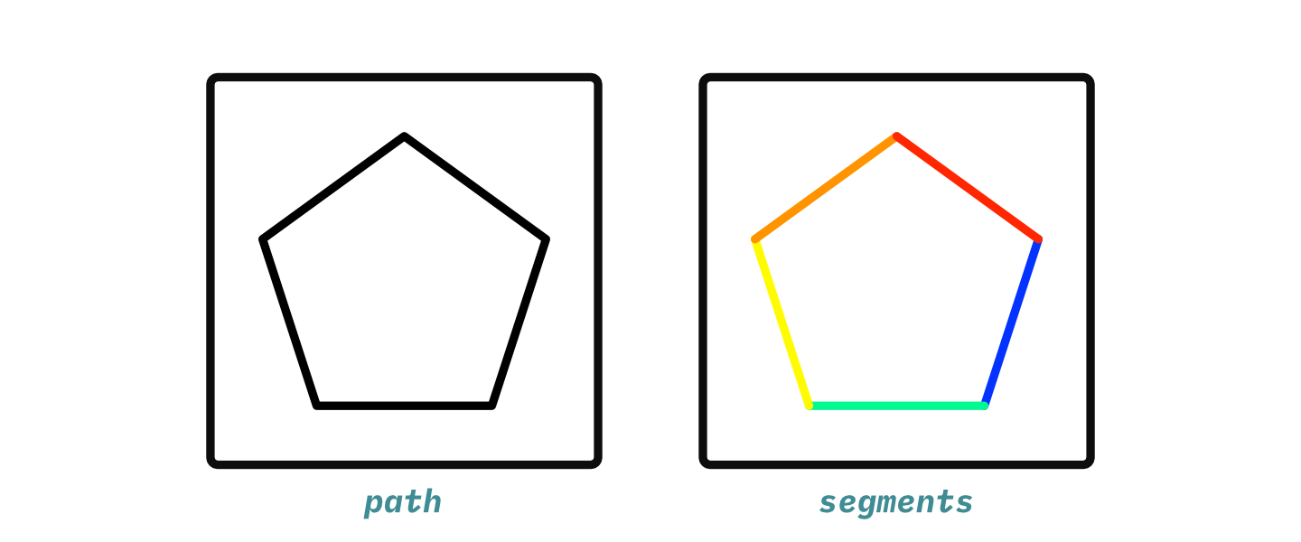
Potrace returns a list of paths. Each path has a list of segments (called curves, though I find that choice in terminology to be a bit confusing):
Polygon generation
Now that the image has been analyzed into a set of paths, the next step is to construct polygons from these paths. While it might seem as simple as iterating through the paths and creating a polygon from its segments, there are a few more hurdles to overcome.
The first is that Potrace path segments can be either lines or cubic Bezier curves:
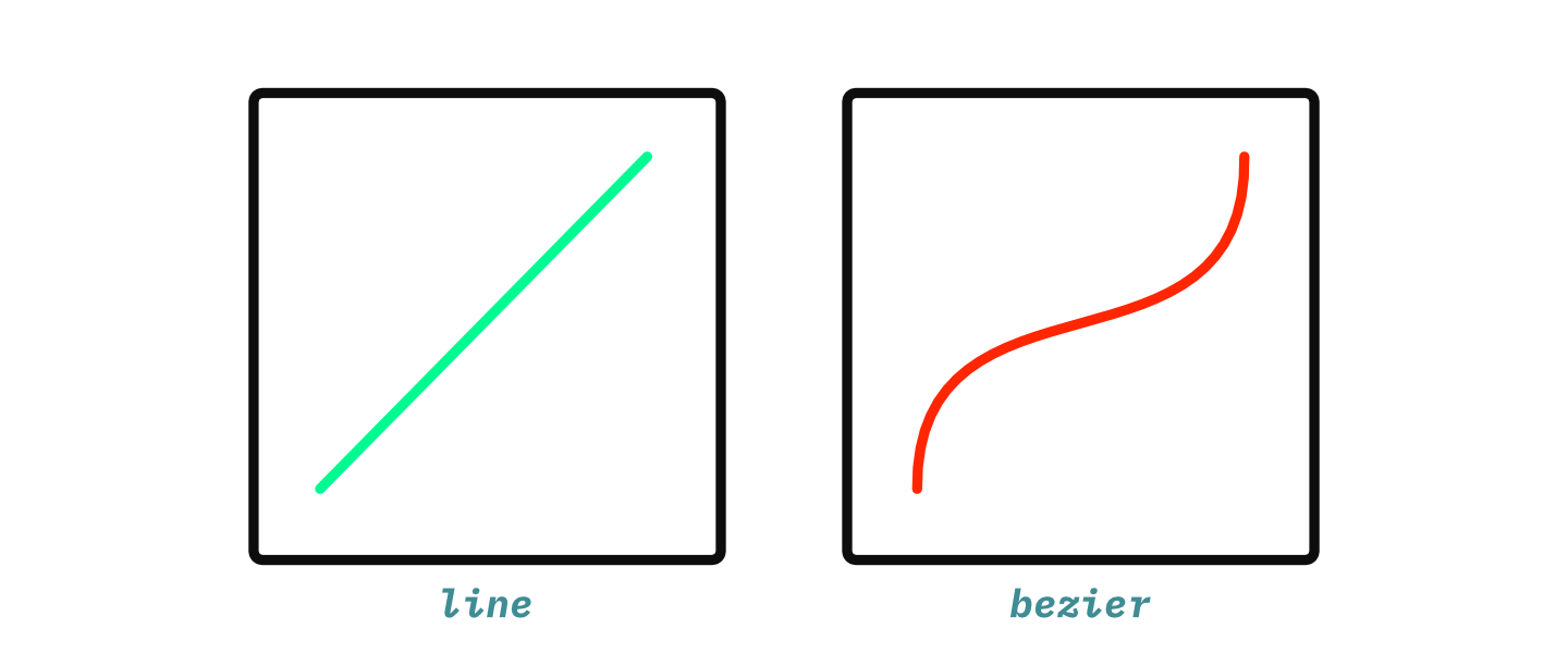
KiCAD's polygons must be a list of points forming line segments, so these Bezier curves need to be approximated by a series of lines. A very, very simple approach is to use a constant number of line segments to approximate the curve3:
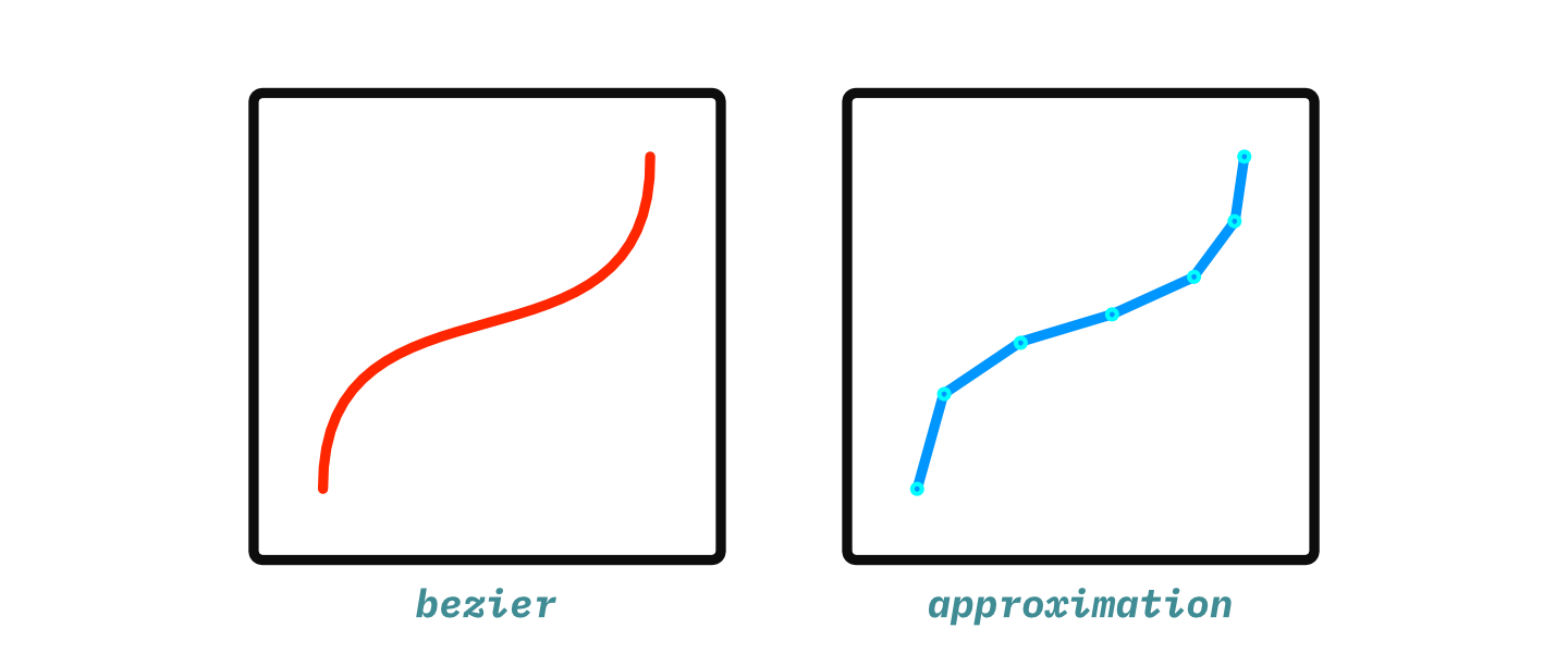
This can be done by evaluating the Bezier formula once for each segment in the approximation:
import math
import numpy

# Type alias for a point
point = tuple[float, float]

def bezier_to_points(p1: point, p2: point, p3: point, p4: point, segments: int = 10):
    for t in numpy.linspace(0, 1, num=segments):
        x = (
            p1[0] * math.pow(1 - t, 3)
            + 3 * p2[0] * math.pow(1 - t, 2) * t
            + 3 * p3[0] * (1 - t) * math.pow(t, 2)
            + p4[0] * math.pow(t, 3)
        )
        y = (
            p1[1] * math.pow(1 - t, 3)
            + 3 * p2[1] * math.pow(1 - t, 2) * t
            + 3 * p3[1] * (1 - t) * math.pow(t, 2)
            + p4[1] * math.pow(t, 3)
        )
        yield (x, y)
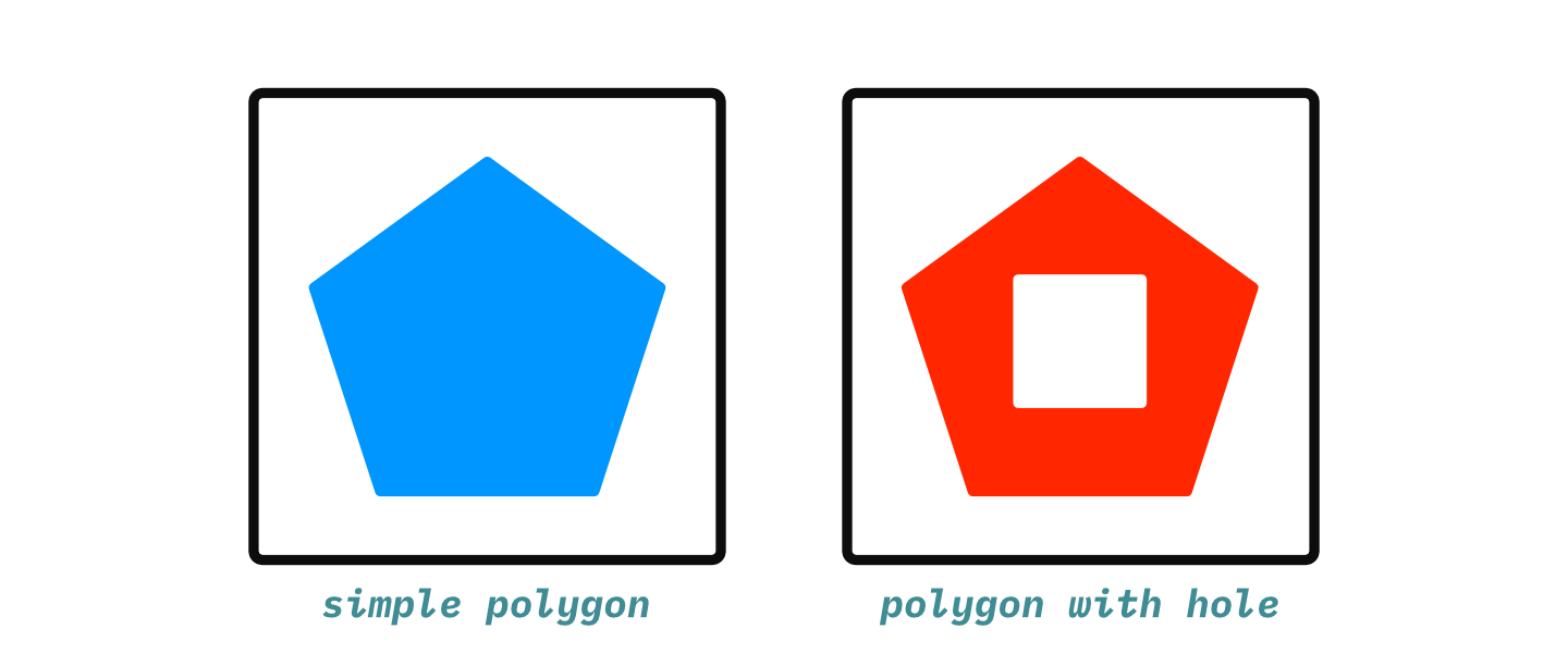
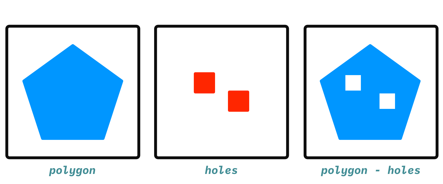
The next obstacle is that KiCAD needs simple polygons- that is, polygons that do not contain any self-intersections or holes. Potrace's paths explicitly do not form simple polygons- they form polygons with holes.
Potrace does offer some help here: each path has a sign. A positive sign indicates that the path is a polygon, while a negative sign indicates a hole. All holes for a given polygon are immediately after it in the list of paths. This can be visualized like this:
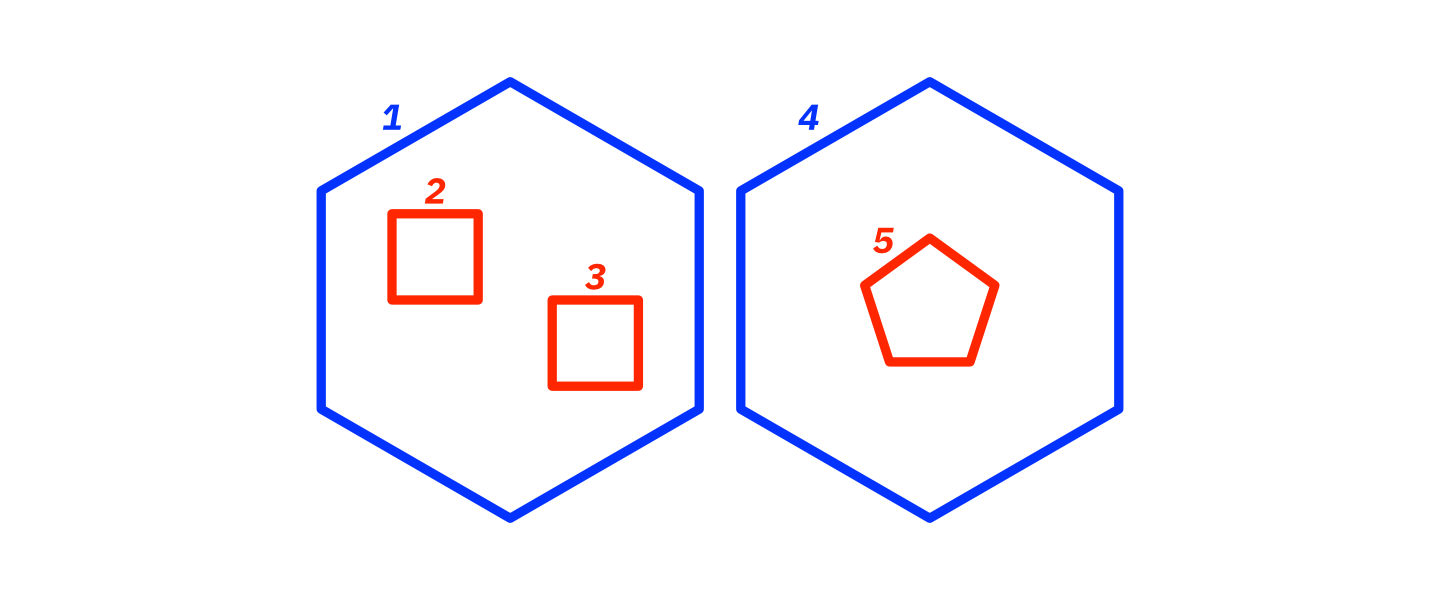
Path 1 is positive (shown in blue) so it is a polygon. The subsequent paths 2 and 3 are negative (shown in red), which indicates that they are holes in the polygon defined by path 1. Path 4 is positive so it indicates a new polygon. Path 5 is negative so it indicates that it's a hole in the polygon defined by path 4.
This information is used to create a list of polygons along with any holes in that polygon. From there, the polygons are "simplified" by subtracting the holes using boolean operations:
Performing polygon operations like this is not for the faint of heart. bitmap2component uses the Clipper library for polygon operations. There are Python bindings for Clipper, but unfortunately I didn't have any luck getting them to work. However, I came across the excellent Gdstk library which has many utilities for working with 2D polygons and uses Clipper behind the scenes. Gdstk also has the great benefit that resulting polygons are simple polygons and don't require any additional processing like dissection2, so they're ready for the journey into KiCAD.
Whew. With all that - a way to convert beziers to line segments, a way to organize the paths into polygons and holes, and a way to simplify the polygons, I can finally get a list of polygons from the Potrace result. This is surprisingly the most complicated code involved here!
First, here's the code for extracting the polygons and holes from the Potrace paths:
import gdstk

# A list that contains lists where the first entry is a polygon and
# any subsequent entries in the list are holes in the polygon.
polygons_and_holes: list[list[gdstk.Polygon]] = []

# Go through each path and pull out polygons and holes
for path in potracecffi.iter_paths(trace_result):

    # Go through each segment in the path and put together a list of points
    # that make up the polygon/hole.
    points = [potracecffi.curve_start_point(path.curve)]
    for segment in potracecffi.iter_curve(path.curve):

        # Corner segments are simple lines from c1 to c2
        if segment.tag == potracecffi.CORNER:
            points.append(segment.c1)
            points.append(segment.c2)

        # Curveto segments are cubic bezier curves
        if segment.tag == potracecffi.CURVETO:
            points.extend(
                list(
                    bezier_to_points(
                        points[-1],
                        segment.c0,
                        segment.c1,
                        segment.c2,
                    )
                )
            )

    polygon = gdstk.Polygon(points)

    # Check the sign of the path, + means its a polygon and - means its a hole.
    if path.sign == ord("+"):
        # If it's a polygon, insert a new list with the polygon.
        polygons_and_holes.append([polygon])
    else:
        # If it's a hole, append it to the last polygon's list
        polygons_and_holes[-1].append(polygon)
Now that the polygons and holes are loaded into gdstk.Polygons, they can be simplified:
# Now take the list of polygons and holes and simplify them into a final list
# of simple polygons using boolean operations.
polygons: list[gdstk.Polygon] = []

for polygon, *holes in polygons_and_holes:
    # This polygon has no holes, so it's ready to go
    if not holes:
        polygons.append(polygon)
        continue

    # Use boolean "not" to subtract all of the holes from the polygon.
    results: list[gdstk.Polygon] = gdstk.boolean(polygon, holes, "not")

    # Gdstk will return more than one polygon if the result can not be
    # represented with a simple polygon, so extend the list with the results.
    polygons.extend(results)
Footprint generation
Alright, the hardest parts are done! The last step is to use those polygons to generate a KiCAD footprint. KiCAD uses a plain-text S-expression format for its files. The S-expression for footprints is:
(footprint "Library:Name"
  (layer "F.SilkS")
  (at 0 0)
  (attr board_only exclude_from_pos_files exclude_from_bom)
  (tstamp "7a7d5548-24ac-11ed-8354-7a0c86e760e0")
  (tedit "7a7d5552-24ac-11ed-8354-7a0c86e760e0")
  [GRAPHICS ITEMS]
)
Other than the basic information4, the important bit is the graphics items. This is where the polygon data will go. Each polygon is represented using an S-expression that contains list of points (pts) where each point is represented using the simple S-expression (xy [X] [Y]):
(fp_poly
  (pts
    [POINTS]
  )
  (layer "F.SilkS")
  (width 0)
  (fill solid)
  (tstamp "7a7d51f6-24ac-11ed-8354-7a0c86e760e0")
)
Here's a simple footprint that puts all these parts together. The polygon inside is just a square, but you can copy and paste this into KiCAD if you want:
(footprint "Library:Name"
  (layer "F.SilkS")
  (at 0 0)
  (attr board_only exclude_from_pos_files exclude_from_bom)
  (tstamp "7a7d5548-24ac-11ed-8354-7a0c86e760e0")
  (tedit "7a7d5552-24ac-11ed-8354-7a0c86e760e0")
  (fp_poly
    (pts
      (xy -10 -10)
      (xy -10 10)
      (xy 10 10)
      (xy 10 -10)
    )
    (layer "F.SilkS")
    (width 0)
    (fill solid)
    (tstamp "7a7d51f6-24ac-11ed-8354-7a0c86e760e0")
  )
)
The only trick here is that KiCAD expects the polygon's points to be in millimeters whereas the points in the polygons extracted from the image correspond to pixels. Up until this point, I haven't considered the physical size of the image. This is generally expressed in terms of dots per inch (DPI) (or pixels per inch)5, but it's easy enough to convert DPI from inches to millimeters:
dots_per_inch = 300
dots_per_millimeter = 25.4 / dots_per_inch
That's the last piece of the puzzle needed to generate the footprint:
def fp_poly(points: list[point]) -> str:
    points_mm = (
        (x * dots_per_millimeter, y * dots_per_millimeter) for (x, y) in points
    )
    points_sexpr = "\n".join((f"(xy {x:.4f} {y:.4f})" for (x, y) in points_mm))
    return f"""
    (fp_poly
        (pts {points_sexpr})
        (layer "F.SilkS")
        (width 0)
        (fill solid)
        (tstamp "7a7d51f6-24ac-11ed-8354-7a0c86e760e0")
    )
    """

poly_sexprs = "\n".join(
    fp_poly(polygon.points) for polygon in polygons)

footprint = f"""
(footprint "Library:Name"
  (layer "F.SilkS")
  (at 0 0)
  (attr board_only exclude_from_pos_files exclude_from_bom)
  (tstamp "7a7d5548-24ac-11ed-8354-7a0c86e760e0")
  (tedit "7a7d5552-24ac-11ed-8354-7a0c86e760e0")
  {poly_sexprs}
)
"""

import pathlib

pathlib.Path("footprint.kicad_mod").write_text(footprint)
The footprint can be copy/pasted or loaded into KiCAD's PCBNew:
Wrapping up
You can reference and try out the full code from this article if you'd like. Note that the code is meant to be educational, so it isn't going to look like production-ready code. You can take a look at gingerbread.trace to see the concepts in this article adapted to a complete tool.
Hopefully this article has given some insight into raster-to-vector conversion and how Python can be used to glue together complex, powerful libraries to accomplish specific goals. While converting a single image to a KiCAD footprint goes a long way towards making PCB art, there is still much more that can be done. In a future article, I'll discuss gingerbread.convert- a powerful tool that can convert an entire design consisting of multiple layers, drills, and complex board outlines.
-
Typically, these are Gerber files for printed circuit boards. ↩
-
KiCAD's bitmap2component calls this fragmentation. ↩
-
KiCAD has a nice adaptive algorithm for this that's based on the overall length of the Bezier curve. I ported this to gingerbread.trace here. ↩
-
I'm ignoring the
tstampandteditfields for now, but they are just UUIDs. ↩ -
300 DPI is common for print design, whereas 72 DPI is common for digital design. In modern design software, DPI is really just a choice of how fine of a resolution you want to work with. ↩